


why you choose us?
-
Senior PCBLayout design team
With more than 10 years of experience in PCB product design, we provide solutions from design to manufacturing. -
10+ years of experience
We have the experience and equipment needed to meet all your advanced PCB needs, from low-cost single-sided PCB to customized multi-layer PCB design and layout services. -
Excellent customer service team
We have a customer service team that provides customers with technical support, production operations and order services 24 hours a day, and can provide technical services online, telephone and e-mail.


OUR PCB design capabilities
- Our full turn-key hardware design services include:
- Board Design and Layout:
- About Hi-Tech Circuit(PCBA)
-
Design idea development, block diagram, power estimate
-
Schematic capture, BOM cost estimate
-
Enclosure/chassis design
-
PCB floor-plan study
-
PCB layout design
-
Thermal/Power Simulation
-
Power Integrity and Signal Integrity analysis
-
PCB fabrication and assembly
-
Board bring-up and testing
-
Hardware user manual, application notes
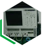
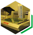
Testing and equipment


Common problems of PCB design
-
1Can I make PCB samples after design?
We have our own PCB and SMT processing factories, which can satisfy customers with one-stop service from design to proofing
-
2How do I charge for PCB design
Generally 3-5RMB/PINS. This price provides invoices, contracts, confidentiality agreements, etc. Specific needs to be evaluated according to the difficulty of the product
-
3What design materials do PCB designs output to customers?
Design data output: PCB source files, Gerber files, assembly files, steel mesh files, structure files, etc.
-
4What does the design process include?
Design specifications, design instructions, customer design requirements and related CHECKLISTs, provide layout files, structure files for customers to conduct layout review; customers confirm the rationality of the layout, stacking scheme, impedance scheme, structure, packaging, and confirm the wiring parameters
-
5What information do I need to provide for PCB design?
The customer needs to provide information: schematic diagram, netlist, structure diagram, device data to be built in the library, design requirements, etc.


